Defect Detection in Transparent Printed Electronics Using Learning-Based Optical Inspection
December 15, 2025 | 928 words | 5min read
Paper Title: Defect Detection in Transparent Printed Electronics Using Learning-Based Optical Inspection
Link to Paper: https://ieeexplore.ieee.org/document/9448191
Date: 08. Jun2 2021
Paper Type: Circuits, Fault Detection, Naural Networks
Short Abstract: Printable electronics is an exciting new technology that allows for the low-cost production of ultra-low-power devices. However, it has two disadvantages: an increased likelihood of manufacturing faults and an increased die size. This increased die size enables optical analysis of the circuit to identify manufacturing faults, which is the focus of this paper.
1. Introduction
Printed electronics are gaining attention because they are flexible, low-cost, and customizable, making them suitable for applications like IoT devices, wearables, RFID tags, and smart sensors. However, printed circuits have lower manufacturing yield than silicon VLSI, making effective testing crucial, yet test costs must remain very low. Traditional electrical testing and design-for-test techniques offer limited observability and are often too expensive, while silicon-style optical inspection and failure analysis are impractical or invasive.
Due to the larger feature sizes, simpler structures, and more transparent layers of printed electronics, low-cost optical inspection using standard cameras becomes feasible. The article proposes a learning-based optical inspection method for detecting gross defects in transparent printed electronics. The approach segments transistor components from optical images, extracts domain-specific features, and compares their performance against standard image-processing features.
Various supervised classifiers, a custom rectangle-based classifier, and an unsupervised KMeans classifier are evaluated to test defect detection and generalization. Results show that domain-specific features detect up to 95% of defective transistors, while standard image-processing features detect only about 40%, demonstrating the clear superiority of domain-specific features. The method also offers insights for failure mode analysis and yield learning in printed electronics.
2. Background on PE
Printed electronics (PE) are a rapidly growing technology, with the market expected to expand significantly from 2019 to 2030. PE enables applications that are difficult or costly to implement with silicon electronics, including photovoltaics, RFID, smart cards, sensor arrays, memory, displays, batteries, wearables, energy harvesting, security primitives, and IoT devices.
Rather than replacing silicon, PE complements it, as it cannot match silicon in performance, integration density, or area efficiency. Its main advantages are low-cost fabrication and the ability to print on rigid or flexible substrates such as plastic or paper using various printing techniques. PE circuits are built using different types of printed transistors, including organic transistors and thin-film transistors. Electrolyte-gated transistors (EGTs) are particularly attractive due to their high mobility and low-voltage operation, enabling low-power applications.
The paper uses EGTs as a proof of concept, though the proposed methodology applies to other printed transistor types.
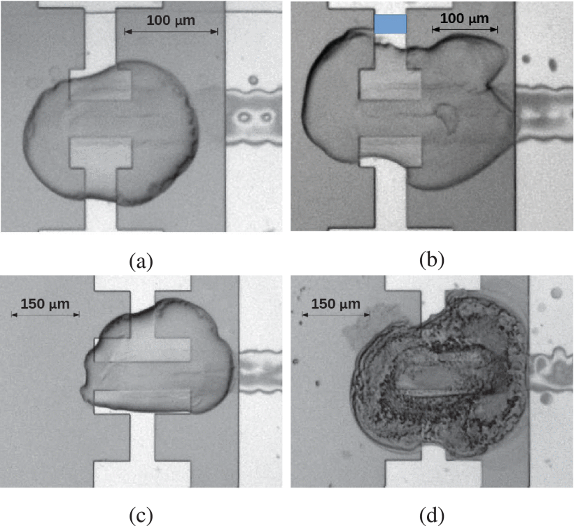
Printed device fabrication involves many process steps, each introducing variation from inks, substrates, and tools. Effects such as wetting issues, droplet irregularities, and missing or satellite droplets lead to high, often non-Gaussian variation in physical and electrical characteristics, resulting in low yield. Despite identical layouts, printed transistors can look physically different, including clearly defective cases.
Because PE feature sizes are in the micrometer range and layers are transparent, low-cost optical inspection using commercial cameras is feasible.
3. Learning based Optical Defect Detection
This section presents a learning-based optical inspection methodology for detecting defective printed transistors, intended as a low-cost replacement for traditional gross defect detection. The approach consists of image preprocessing, feature extraction, feature evaluation, and generalization analysis.
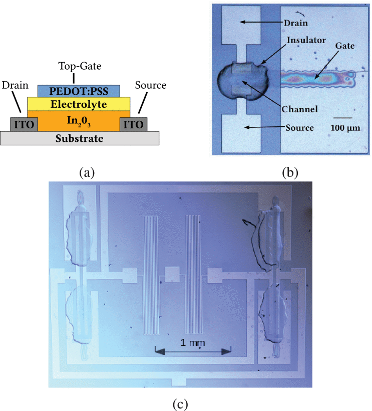
First, microscope images are preprocessed to reduce noise, normalize intensity, correct rotation, and align regions of interest. Images are converted to grayscale, rotated using a Hough-line–based reference, normalized, denoised, contrast-enhanced, and binarized. Template matching is then used to locate a common reference (the drain electrode) so images can be cropped to a uniform size.
Next, transistor parts are segmented to enable domain-specific feature extraction. The electrolyte is segmented using Chan–Vese segmentation followed by flood fill, erosion, and region labeling. The right part of the top-gate electrode (RPTGE) is segmented using Canny edge detection, Hough transforms, and flood fill. Based on these segments, two types of features are extracted:
- Domain-specific features, computed on segmented transistor parts (electrolyte and RPTGE), capturing material density, shape, coverage, alignment, and potential electron-flow bottlenecks.
- Standard image-processing features, computed on the whole image without segmentation.
Domain-specific features include statistical measures (mean, variance, entropy), electrolyte–gate distance or overlap, electrolyte coverage of source/drain electrodes, electrolyte area, and shape/intensity moments, all of which relate to physical transistor behavior.
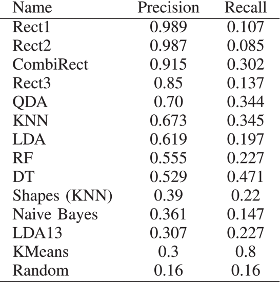
Feature quality is analyzed using scatterplot matrices for low-dimensional features and t-SNE for high-dimensional ones. To assess generalization to unseen data, multiple classifiers are evaluated: supervised methods (DT, RF, LDA, QDA, Naive Bayes, KNN), an unsupervised method (KMeans), and a custom rectangle classifier. Extensive cross-validation is performed, comparing domain-specific features with standard image features while accounting for limited data and the curse of dimensionality.
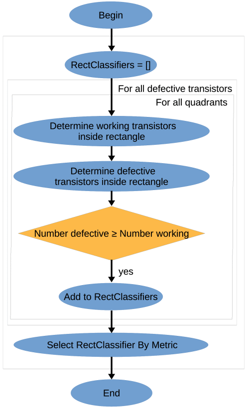
The rectangle classifier exploits feature-space regions where defective transistors cluster, defining rectangles around defective points that preferentially include more defects than working devices. These rectangles can be combined or selected to maximize defect detection while minimizing false positives.
4. Evaluation
5. Conclusion
As optical inspection is feasible for PE due to the bigger feature sizes, transparent layers, and smaller number of layers compared to silicon-based electronics, it is possible to avoid electrical testing for gross manufacturing defect detection in PE. ith the domain-specific features, it is possible to detect 95% of the defective transistors correctly, whereas for the standard image processing fea- tures, it is 40%.
 reply via email